※ 학부 수준의 글이므로, 내용에는 오류나 부족한 부분이 있을 수 있습니다. 이에 대한 지적이나 수정 제안을 환영하며, 더 정확하고 명확한 내용으로 보완하겠습니다. 더 자세한 설명이 필요한 부분이 있다면 언제든지 알려주시면 감사하겠습니다.
-2D TMDCs (two dimensional metal dichalcogenides)
: MoS2, MoSe2. WS2

>layer to layer distance 0.65nm
>tunability in band gaps between 1.0~2.0eV
-single layer (direct bandgap)
: MoS2 1.8eV, MoSe2 1.5eV
-bulk (indirect bandgap)
: MoS2 1.2eV, MoSe2 1.1eV
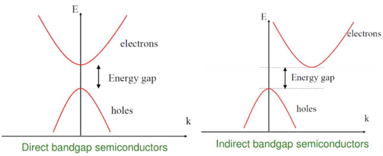
*direct bandgap
: maximum energy level of the valence band aligns with the minimum energy level of the conduction band with respect to momentum
: 빛 energy 방출하며 conduction band에서 valance band로 내려옴
*indirect bandga
: maximum energy level of the valence band and the minimim energy level of the conduction band are misaligned with respect to momentum
: 수직 방향으로 내려올 때는 빛 energy, 사선으로 내려올 때는 열 energy 방출하며 conduction band에서 valance band로 내려옴
: energy 일부를 열 energy로 방출하면서 효율성이 떨어짐
(참고: http://edetec106.blogspot.com/2016/01/differentiate-between-direct-and.html)
>vertically stacked
>weakly interacting layers (van der Waals)
*van der waals force
: the force are due to the attractions between the partial positive and partial negative electrical charges between molecules / 원자 사이 발생하는 인력, 척력
: these foreces are affected by the distance between the molecules
(closer magnet, greater attraction)
(참고: https://www.expii.com/t/van-der-waals-forces-definition-overview-8350)
>yielding devices with low off current
>on/off ratio above 10^6
>high-field-effect mobility
>60mV/decade subthreshold swings
-1/f noise (flicker noise)
: inverse of the signal's frequency
: significant for low-frequency signals

αH = Hooge parameter
Nc = number of charge carriers in the conductor
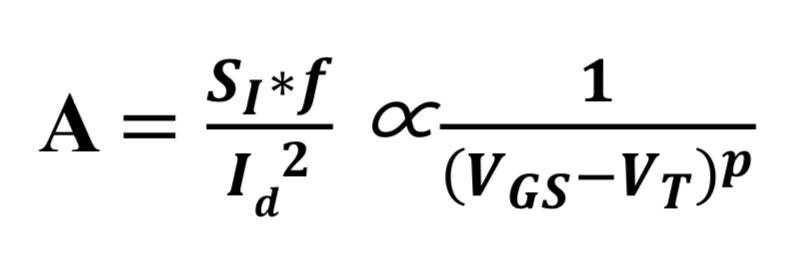
SI = power spectral density of current noise
f = frequency
p = factor
(p=1 / mobility fluctuations, Hooge model)
(p=2 / number fluctuation, McWhorter's model)

(hooge model (p=1)인 경우 McWhorter's model(p=2)에 비해 그래프가 완만하게 형성됨)
-Extrinsic and Intrinsic
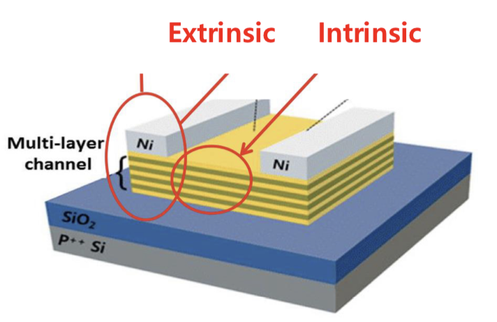
extrinsic : contact / access region
> interlayer coupling
> resistance arising from SD contact
intrinsic : channel region
> carrier scattering
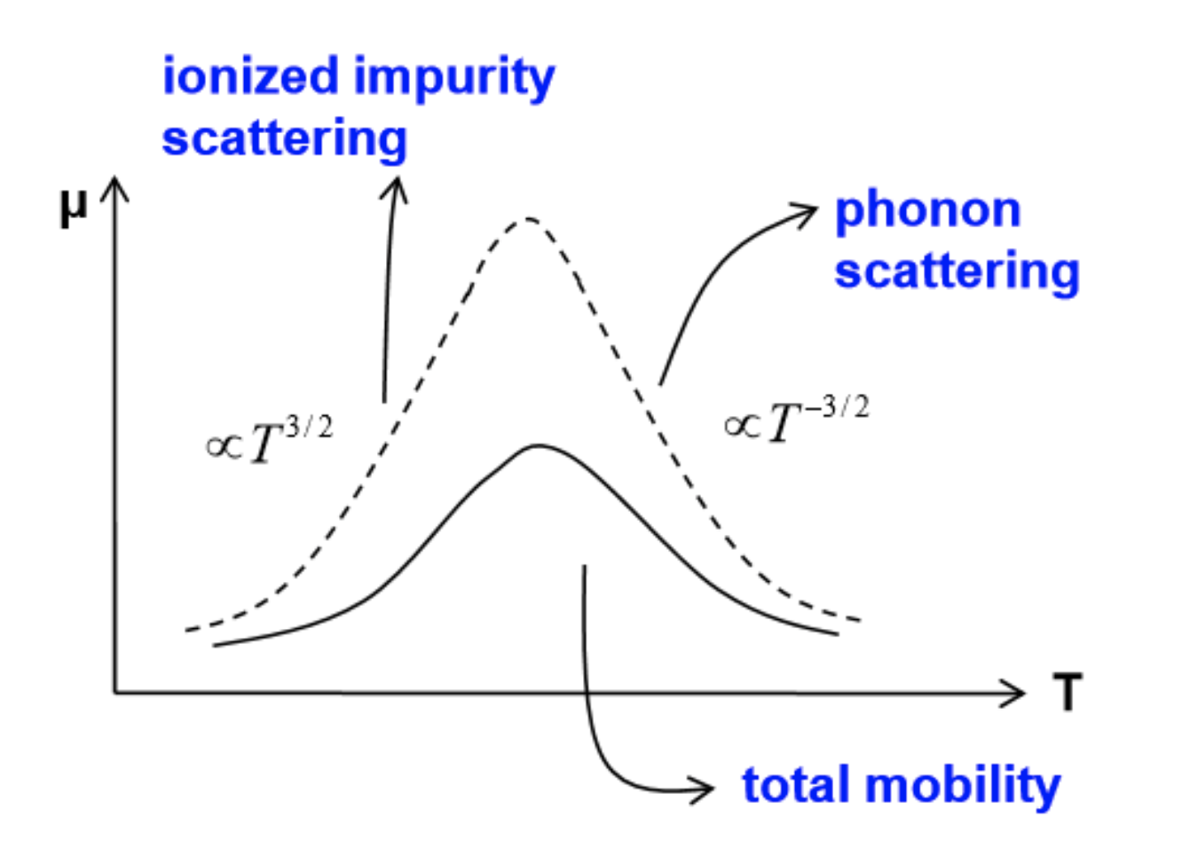
*carrier scattering
> Lattice scattering (phonon scattering)
: Si 원자 자체의 진동 (phonon)으로 인한 불균형 발생
: 300K (room temp)일 경우 포함함
: high temp > more scattering > low mobility
>Impurity scattering
: donor의 경우 hole을 밀어내고, electron을 끌어옴
: acceptor의 경우 electron을 밀어내고, hole을 끌어옴
: 불순물에 의해 전자/정공의 원래 운동을 방해해 속도가 감소
: high impurity (high doping) > more scattering > low mobility
: high temp > low impurity impact > less scattering > high mobility
(참고: https://jehunseo.tistory.com/46)

x-axis : doping concentration
y-axis : mobility
-Schottky barrier
: the energy difference between the valance (or conduction) band edge of semiconductor and the Fermi energy band of the metal
: 금속-반도체 juction에 형성된 전자에 대한 potential energy barrier
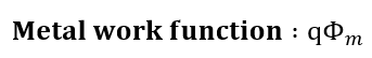
*work function
: minimum energy required to a free electrons to come out of the metal surface
: metal에 빛을 쪼이면 특정 주파수보다 높은 경우 전자가 진공으로 튀어나오게 되고, 이때 전자가 진공으로 튀어나오는 minimum energy
(참고: https://byjus.com/question-answer/define-work-function-of-a-metals/#)

*fermi-level
: probability of finding carrier
: energy level where there is a 50% chance of finding e-
*electron affinity
: semiconductor에서 fermi-level에 전자가 갈 수 있는 state이 존재하지 않아, vacuum의 energy level과 전자가 갈 수 있는 state인 conduction band의 energy level의 차이
: 즉, 반돋체에 빛을 쪼였을 떄, 전자가 나오는 minimum energy
(참고: https://m.blog.naver.com/cj3024/221294774519)


*ohmic contact, schottky contact
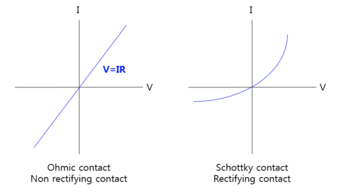
*ohmic contact
: low resistance ohmic contacts are used to allow charge to flow easily in both directions between the two conductors, without blocking due to rectification or excess power dissipation due to voltage thresholds
: I-V curve 따름
(참고: https://en.wikipedia.org/wiki/Ohmic_contact)
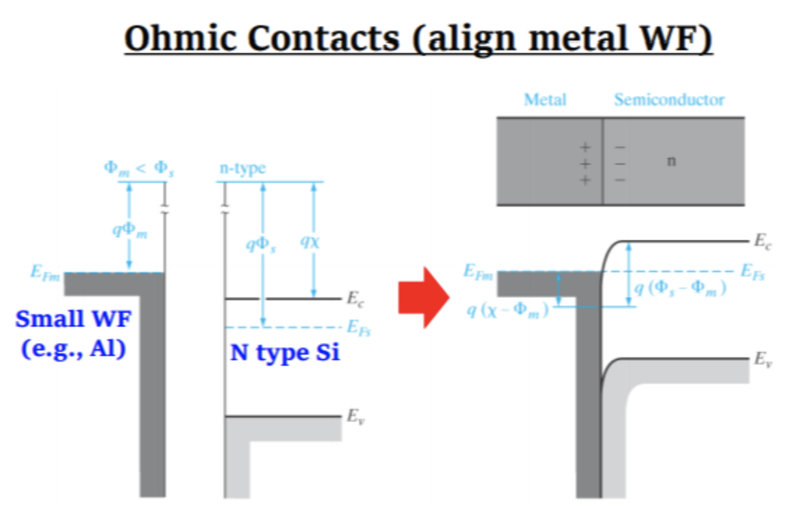
-n-type (metal work function < semiconductor work function)
-p-type (metal work function < semiconductor work function)
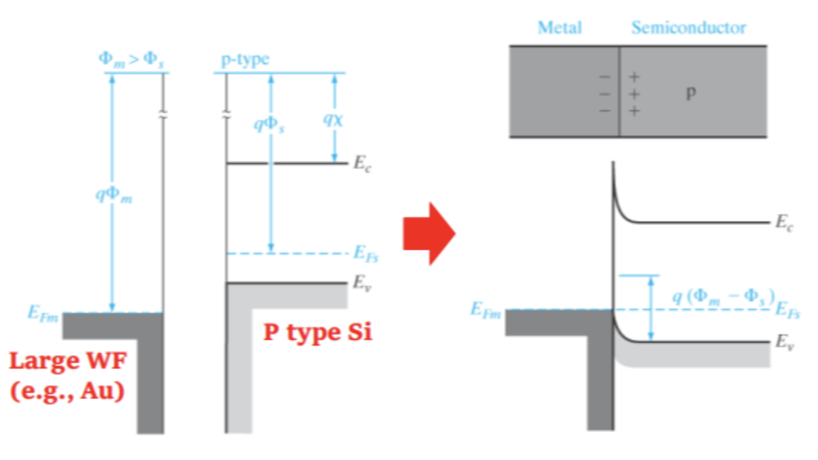
(pn junction의 개수를 줄이고자 metal-semiconductor contact 부분에서는 ohmic contact이 형성될 수 있도록 heavy doping 해줌)
heavy doping
: depletion region의 폭이 좁아져 schotty barrer를 tunneling에 의해 metal to semiconductor로 넘어갈 수 있게 되면서 양방향으로 전류가 흐를 수 있게 된다
*schottky contact
-n-type (metal work function > semiconductor work function)
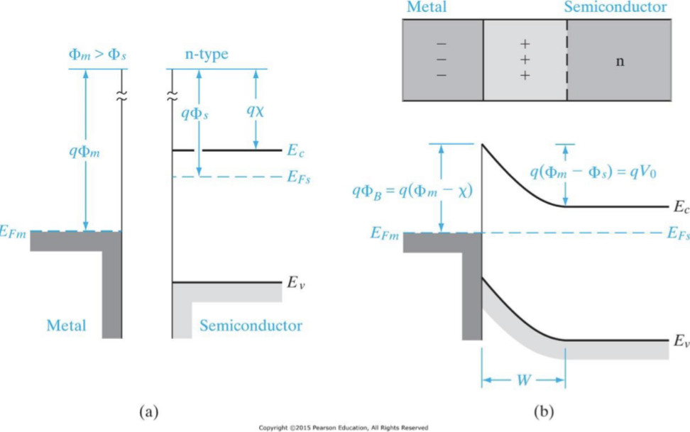
(n-type electron이 schotty barrier height를 뛰어 넘기 어려움)
-p-type (metal work function < semiconductor work function)

(p-type hole이 schotty barrier height를 뛰어 넘기 어려움)
(reverse bias 걸어주면 schotty barrier height이 더 커져 전류 흐르기 더 어려워짐)